All sciences. №9, 2023. International Scientific Journal
This phenomenon is caused by a decrease in the amplitude A1 of the main attenuation mode with an effective excitation depth, which is the inverse of the absorption coefficient α [2]. The absorption coefficient increases sharply with the energy of the excitation photon at the absorption edge of the CdTe material in the wavelength range of about 800—1000 nm [4]. At the same time, the dependence of the absorption coefficient on the layer thickness inherent in CdTe nanostructures [5] can be ignored, since the layer thickness of 1 µm is sufficient to have the properties of a bulk material.
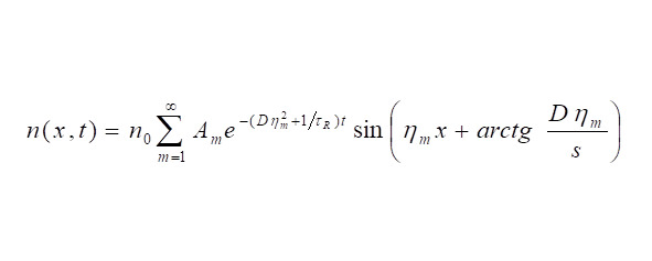
The change in carrier density over time t along the plate depth coordinate x is described by the ratio

where is the concentration of excess carrier pairs introduced by light, is the attenuation amplitude attributed to the spatial frequency m of the decay mode, is the lifetime of volumetric recombination, is the coefficient of ambipolar diffusion of carriers, is the rate of surface recombination.

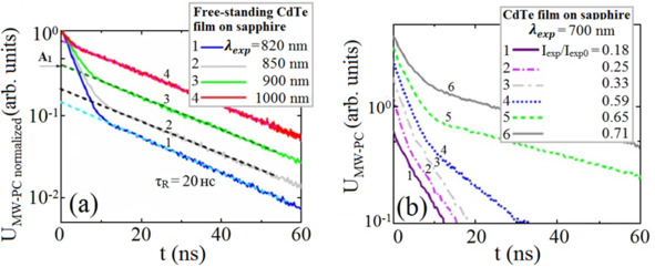
Fig. 2. (a) Change in the excitation wavelength (at low excitation values I1/I2=0.2) – (b) the excitation density (at 700 nm) of MW-PC transient-dependent processes recorded at T = 300 K in a CdTe film mounted on a sapphire.
From the amplitude of the transients, it follows that with homogeneous excitation, the recombination processes will be linear (Fig. 2.b), while the decay of carriers in the initial phase indicates a non-exponential attenuation process in inhomogeneous excitation (Fig. 2.a).
Inherent in a number of transients determined by surface recombination and obtained for different excitation depths (Fig. 2.a) is an almost constant effective lifetime in the phase of asymptotic attenuation (considered as the same attenuation slope in Fig. 2.a), the value of 19 ns was determined [2].
An increase in the excitation intensity leads to an increase in the relative amplitude of the asymptotic attenuation component with inhomogeneous excitation of 700nm (Fig. 2.b). This hints at the rate of surface recombination, depending on the concentration of excess carriers.
This result is easy to understand if we assume that the filling of most surface traps is saturated. In experiments, when the highest excitation densities were used, it led to a decrease in the rate of surface recombination to values of 5 · 106 cm/s.
Summing up the analysis of the results, it is shown that the spectral photosensitivity of the CdTe layer in terms of short – circuit current and photo EMF can be controlled by the induced built – in electric charge of the dielectric created by the external potential of the corona discharge and the heterostructure of CdTe (film) – SiO2 (dielectric) – Si (semiconductor) – Al (aluminum).
This opens up new possibilities for the creation of semiconductor devices sensitive to electromagnetic radiation, which are also used in optoelectronics as a photosensitive device with a spectral characteristic in a wide sensitivity range. This effect is also associated with fundamentally new capabilities of semiconductor devices with variable spectral characteristics and matching it with an emitter, which is important for devices and information recording systems.
Literature
[1] Gaubas E., Čeponis T., Vaitkus J.V., Pulsed Capacitance Technique for Evaluation of Barrier Structures, LAMBERT Academic Publishing, Saarbrucken-Berlin, 2013 (ISBN:978-3-659-50518-8).
[2] Gaubas E., Simoen E., Vanhellemont J., Review – carrier lifetime spectroscopy for defect characterisation in semiconductor materials and devices, ECS J. Solid State Sci. Technol. 5 (2016) p.3108—3137.
[3] Lucovsky G., On the photoionization of deep impurity centers in semiconductors, Solid State Commun. 3 (1965) p.299—302.
Конец ознакомительного фрагмента.
Текст предоставлен ООО «Литрес».
Прочитайте эту книгу целиком, купив полную легальную версию на Литрес.
Безопасно оплатить книгу можно банковской картой Visa, MasterCard, Maestro, со счета мобильного телефона, с платежного терминала, в салоне МТС или Связной, через PayPal, WebMoney, Яндекс.Деньги, QIWI Кошелек, бонусными картами или другим удобным Вам способом.
Вы ознакомились с фрагментом книги.
Для бесплатного чтения открыта только часть текста.
Приобретайте полный текст книги у нашего партнера:
Всего 10 форматов